By carefully controlling oxygen exposure during fabrication, scientists at Stanford University have created field-effect transistors (FETs) out of two-dimensional semiconductors. The transistors are atomically thin and benefit from “native” high-k dielectrics, which can enable low-defect interfaces and low-power operation. The researchers believe that such devices could help overcome current limitations imposed by power dissipation in modern electronics.
Silicon has maintained a strong hold on integrated electronics for more than five decades. This material’s moderate band gap minimizes leakage currents and provides the ability to switch transistors “off”, minimizing power consumption. Silicon also readily accepts dopants to form p-n junctions, enabling the creation of solar cells and complex circuits. In addition, unlike many other semiconductors, silicon benefits from the existence of silicon dioxide (SiO2), a robust and native insulator, allowing for good electrical isolation between silicon components.
Despite the factors in silicon’s favour, incremental improvements in processor performance are becoming harder to come by. Historically, transistor density has grown exponentially, bringing with it increased computing power. However, as transistor dimensions have entered the nanoscale regime, quantum effects such as tunnelling have begun to dominate the total power consumption. In the past decade, performance improvements have been driven less by Moore’s law and more by design innovations including the use of strain and the replacement of traditional silicon dioxide with high-k dielectrics like hafnium oxide (HfO2).
Beyond silicon
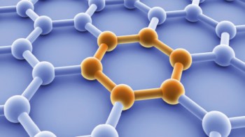
Now, Michal Mleczko, Eric Pop and colleagues at Stanford University have fabricated field-effect transistors based on hafnium and zirconium diselenides (HfSe2 and ZrSe2) – semiconductor materials formed from “two-dimensional” crystal layers three atoms thick. These materials exhibit band gaps comparable to that of silicon even at single-layer thicknesses, enabling the design of atomically thin electronics.
Inspired by the need for native insulators in good semiconductors, the Stanford researchers looked for the formation of HfO2 and zirconium oxide (ZrO2), which would fulfil the role played by SiO2 in silicon-based miroelectronics. Transmission electron microscopy (TEM) images taken by the researchers showed that HfSe2 and ZrSe2 readily form such native oxides when exposed to oxygen. Furthermore, the oxides are the same high-k dielectrics that have been painstakingly implemented in silicon electronics for the past decade. The use of naturally forming oxide produces interfaces between the semiconductor and the insulating layer that have low defect density.
The researchers prepared transistors using the native oxides (HfO2, ZrO2) or a non-native insulator (aluminium oxide, Al2O3), which was deposited separately. To directly compare the performance of the transistors, the current was measured as a function of gate voltage, illustrating how otherwise identical devices behave. These measurements revealed that the devices with high-k dielectrics exhibited much lower defect densities at the semiconductor–dielectric interface.
A significant challenge moving forward comes from the tendency of these two semiconductor materials to form oxides too readily, as this happens spontaneously in the presence of ambient oxygen. Furthermore, oxygen atoms diffuse through the oxide crystal lattice, meaning that the oxide growth is not self-limiting. The need to prevent inadvertent exposure to oxygen in the ambient environment posed a big hurdle during device fabrication: devices and samples had to be kept in nitrogen gas or under vacuum to inhibit unintentional excess oxide formation. Left unchecked, the oxidation process could consume the entire semiconductor sample, akin to the rusting of a metal.
Full details of the research are reported in Science Advances 10.1126/sciadv.1700481.