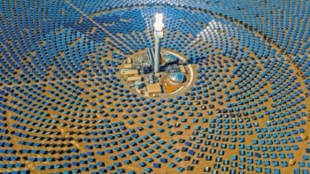
The voltage of Cu2ZnSn(SxSe1−x)4 (CZTSSe) kesterite solar cells has so far limited their efficiency. But by carefully tweaking the composition of CZTSSe, Priscilla Antunez along with her co-workers at IBM’s TJ Watson Research Centre, have shown that the voltage output of these solar cells can be dramatically increased. This result has roused a great deal of excitement at IBM as these cells are ideal for powering the autonomous appliances that will constitute the Internet of Things.
Sulphurization boosts voltage
When solar cells are illuminated, a potential difference builds up as electrons and holes are separated across the semiconductor band-gap. By widening this gap, scientists can increase the voltage available to power a given appliance.
This principle has been manipulated by researchers working on CZTSSe for some time now, as increasing the ratio of S/Se shrinks the crystal lattice and widens the band-gap. Nevertheless, though scientists observe an increase in voltage using this method, it is accompanied by a deterioration of the device electronics, resulting in up to 3% lower efficiency.
The problem stems from the vigorous 600 °C “hot-bake” method used to add extra S into the system. The extreme temperatures facilitate the formation of Mo(S,Se)2 at the interface between the kesterite and the molybdenum substrate. Mo(S,Se)2 impedes the movement of charge-carriers to the electrode and is the key cause of power loss.
Exfoliation improves electronics
But now, researchers at IBM have developed an ingenious exfoliation process in which the essential “hot-bake” proceeds as normal and the undesirable Mo(S,Se)2 layer is simply cleaved off along with the substrate. The device is then completed by adding a more appropriate back contact to the exposed CZTSSe surface.
The implications of this development for kesterite device performance are massive. Firstly, by increasing the S/Se ratio the researchers managed to drastically improve the cell voltage by roughly 30%. But most importantly, they could do this without tarnishing the integrity of the kesterite crystal structure. Indeed, the removal of Mo(S,Se)2 from the film meant that overall device efficiency dropped by only 1%, as opposed to the 3% observed in previous studies.
Powering the Internet of Things
But it is not just this result that has piqued the interest of those at IBM. A large barrier to the full-scale implementation of the autonomous, and importantly, wireless appliances that will make up the Internet of Things, is how to power them. Individual devices will need to harness energy from their environment and so photovoltaics will undoubtedly play a key role here.
Crucially, many of these devices will operate inside at low light levels. Most commercial solar-cell technologies typically exhibit a 2–3 times reduction in efficiency upon moving from direct sunlight (1 sun) to indoor lighting (< 0.01 suns). But the IBM researchers have shown that CZTSSe exhibits only a marginal drop in efficiency at these light levels, while maintaining a reasonable voltage. Critically, the voltage of a monolithic nine-cell series connected device was found to be 2 V under office-lighting conditions – more than enough to power a typical microprocessor used for autonomous applications. This staying power could make kesterite photovoltaics the ideal candidate for powering the trillions of connected appliances that will make up the Internet of Things.
Further details can be found in Nature Energy.