 Astronomy and space
 Atomic and molecular
 Biophysics and bioengineering
 Condensed matter
 Culture, history and society
 Environment and energy
 Instrumentation and measurement
 Materials
 Mathematics and computation
 Medical physics
 Optics and photonics
 People
 Quantum
 Scientific enterprise
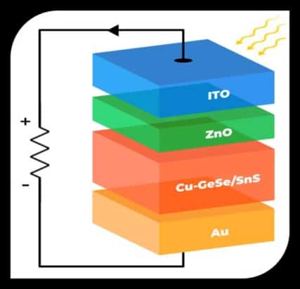
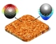
Material contains special bandgap states that efficiently absorb light at crucial solar wavelengths
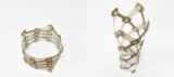
Research could lead to the development of electrolytic computers
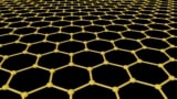
 Read article: Local twist angles in graphene come into view
Scanning microwave impedance microscopy technique could help scientists better understand materials like twisted bilayer graphene
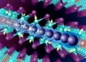
 Read article: Bacterial nanowires make an electrical grid in the soil
Anaerobic bacteria depend upon a single family of proteins to transfer extra electrons they produce to electric hairs on their surface
 Read article: Roll-to-roll-fabricated hybrid perovskite solar cells reach record efficiencies
Researchers calculate that large-scale devices would be cheap to produce, too
 Read article: Quasiparticles called merons appear in a synthetic antiferromagnet for the first time
Collective topological chiral spin textures could lead to new concepts for spintronics devices
 Read article: Sticky materials un-stick themselves in jumps
New work could change the way we think about how soft materials adhere to surfaces
 Read article: New metamaterial could make true one-way glass
Theoretically proposed structure could also improve the efficiency of solar cells
The 2024 edition of Physics World Careers is packed full of advice for early-career scientists. Including a range of valuable advice, informative case studies and recruiter profiles, it demonstrates the variety of jobs that use a physics degree.
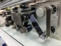
 Read article: Battery cyclers: shedding light on the detail of electrochemical materials and devices
High-performance battery cyclers offer reliable, accurate and repeatable test sequences in R&D and production settings
 Read article: Combining electrochemistry and neutron reflectometry in situ
The Electrochemical Society tells you more about the unique data obtainable by combining electrochemistry and neutron reflectometry in situ
 Read article: Solid-state battery electrolyte makes a fast lithium-ion conductor
New material allows lithium ions to move in 3D and could compete with liquid electrolytes in mainstream Li-ion battery technologies
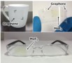 Read article: Sticky UV-sensitive tape makes 2D material transfers easier
New technique could help integrate materials such as graphene into real-world devices
 Read article: Electrochemical atomic force microscopy of battery interfaces
The Electrochemical Society explores an in-depth understanding of electrochemical atomic force microscopy in battery interfaces
 Read article: Surface ‘signature’ could distinguish exotic topological insulators
Changes in the polarization of light reflecting off a material’s surface could indicate whether it is a higher-order topological insulator, say theorists
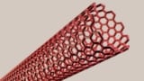 Read article: Carbon nanotubes make optical sensor flexible and ultrathin
Device works across electromagnetic spectrum from terahertz to visible
 Read article: Nanoparticles enhance locusts’ sense of smell
Research could lead to better chemical sensor
 Read article: Monocrystalline gold brings electronic devices near the efficiency limit
The absence of grain boundaries significantly improves how long “hot” electrons hold onto their high energies and how easily they can be exploited
 Read article: Collapsible helix antenna could aid disaster recovery
New device switches between two operating modes as it is extended and contracted and might also be deployed in space
 Read article: Graphene-based materials show great promise for hydrogen transport and storage
Materials expert Krzysztof Koziol also talks about hydrogen-powered aircraft
 Read article: Heavy fermions appear in a layered intermetallic crystal
New two-dimensional compound could be used to study interactions that produce unconventional superconductivity and related quantum phenomena
 Read article: Shallow defects drive slow recombination, high efficiency in perovskite solar cells
Findings could help improve cell efficiencies still further, say physicists
 Read article: Semiconductor fibres are fracture free and glass clad
New process could yield flexible and wearable optoelectronics
 Read article: Long-lived qubits survive as ‘islands’ in a noisy environment
Discovery could aid the development of quantum computing architectures in which qubits are implanted randomly into a host matrix
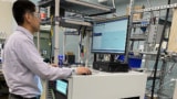
 Read article: AI tools for materials research and nanotechnology
IOP Publishing's journal, Nano Futures, explores the rapidly progressing field of intelligent nanotechnology
 Read article: Hair helps keep us cool in hot weather, infrared study reveals
Longer wavelength radiation is emitted easily by hair
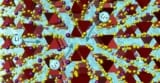
 Read article: Snapshot of noble gas atoms emerges from within a graphene sandwich
Nanoclusters of krypton and xenon directly imaged at room temperature for the first time thanks to confining layers of graphene